
Description
Patterning is the process of defining precise geometric shapes on a substrate to build the layered structures that make up microelectronic, Micro-Electro-Mechanical-Systems (MEMS), or photonic devices. It is a core step in microfabrication that allows selective addition, removal, or modification of materials on the wafer.
What We Offer
We offer a wide range of techniques and materials for patterning. Our capabilities include photolithography and shadow masking. We work with both positive and negative photoresist, image reversal, lift-off processes, and dry film resist with thicknesses exceeding 100 microns. Aside from common resist, we also work with materials such as SU-8, benzocyclobutene (BCB), and polyimide.
Materials
- Positive photoresist
- Negative photoresist
- Lift-off resist
- Polyimide
- SU-8
- Benzocyclobutene (BCB)
- Dry film resist
Patterning Techniques
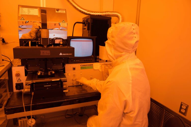
Photolithography
A light-sensitive material called photoresist is deposited on a substrate and selectively exposed to UV light through a mask that defines the desired pattern. After exposure and development, portions of the photoresist remain (or are removed), forming a mask on the substrate for further processing.
We offer a full suite of capabilities related to photolithography, such as contact aligners, programmable spinners, hexamethyldisilazane (HMDS) ovens, image reversal ovens, spin-rinse machines, automated photomask cleaner, oxygen (O2) plasma descum and stripper, developing station, lift-off station, and resist strip station.
Our in-house workhorse processes utilize contact aligners that are capable of patterning large area substrates. For submicron feature sizes, we utilize projection aligners and e-beam lithography tools at nearby offsite facilities.
Dry film processing
Dry film processing refers to the use of solid, photosensitive polymer sheets that are laminated onto substrates and patterned using photolithography. Unlike liquid resists, dry films are pre-cast, offering uniform thickness, clean handling, and easy lamination. The process allows patterning of substrates with large thru-hole vias.
We offer extensive experience with dry film photoresist, including patterning large and odd-shaped substrates containing large thru-hole vias. We can define and align structures on back to back substrate surfaces. We also know how to work with photoresist that are over 100 microns thick to, for example, form patterned metals over 140 microns thick.
Lift-off processing
Lift-off is a patterning technique used to define thin film features by depositing material through a patterned resist mask and then removing the resist along with the unwanted material on top of the resist. Unlike etching, which removes material after blanket deposition, lift-off avoids exposing the substrate to aggressive etchants. The technique is especially useful for patterning multi-layer metal or dielectric stacks that are difficult to etch.
We have extensive experience with lift-off processes. These include deploying specialized bilayer lift-off resists or using single layer resist formed to realize retrograde sidewall profiles. We perform lift-off on large full wafers, as well as on small cm-size coupons.