Description
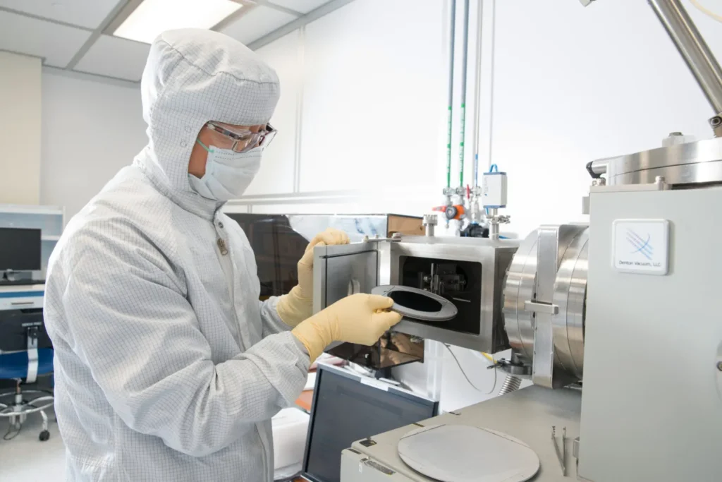
Thin film deposition is a critical process in microfabrication used to create layers of materials, typically in the nanometer to micrometer thick range. These layers can serve various functions, such as insulation, conduction, light reflection, light-emission, light detection, or as a structural component. Deposition methods include physical vapor deposition such as sputtering and evaporation, chemical vapor deposition, epitaxy, and electroplating. The choice of technique depends on the required film properties, such as stress, adhesion, refractive index, density, thickness, and composition. Thin films are foundational in the manufacturing of semiconductors, Micro-Electro-Mechanical-Systems (MEMS), and other micro-scale devices.
What We Offer
We offer comprehensive thin film deposition services, including a wide range of materials and techniques to suit your needs. Whether you require simple single-layer films on your chosen substrate or process development to determine the optimal materials and methods for your device, we can support you at every stage.
Materials
A wide range of materials can be used in thin film deposition, including metals, dielectrics, and semiconductors. The choice of material depends on the intended function of the film. Conductive films are typically metals, insulating layers use dielectrics, and semiconducting films use doped or intrinsic semiconductor materials. Selection is guided by factors such as electrical, optical, thermal, and mechanical properties, as well as compatibility with other process steps and substrate materials. Deposition conditions and techniques are often tailored to optimize these properties and ensure uniformity, compatibility, and stability of the film in the final device structure.
Our thin film deposition offering includes the following thin film materials:
- Titanium (Ti)
- Platinum (Pt)
- Gold (Au)
- Nickel (Ni)
- Germanium (Ge)
- Paladium (Pd)
- Gold (Ag)
- Copper (Cu)
- Chrome (Cr)
- Tungsten (W)
- Ti-Tungsten (TiW)
- Molybdenum (Mo)
- Moly-Chrome (MoCr)
- Niobium (Nb)
- Aluminum (Al)
- Silicon Dioxide (SiO2)
- Silicon Nitride (Si3N4)
- Silicon Oxinitride (SiON)
- Aluminum Oxide (Al2O3)
- Titanium Dioxide (TiO2)
- Yttrium Fluoride (YF3)
- Tantalum Pentoxide (Ta2O5)
- Silicon Carbide (SiC; Physical Vapor Deposition – PVD)
- Indium (In)
- Silicon (Si)
- Amorphous Silicon (a-Si)
- Polysilicon (Poly-Si)
- Indium Tin Oxide (ITO)
- Gallium Arsenide (GaAs) heterostructure
- Indium Phosphide (InP) heterostructure
- Gallium Nitride (GaN) heterostructure
- Aluminum Nitride (AlN) heterostructure
- Gallium Antimonide (GaSb) heterostructure
Deposition Techniques
Sputtering
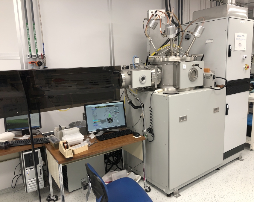
Sputtering is a physical vapor deposition (PVD) technique used to deposit thin films by ejecting atoms from a solid target material using energetic ions, typically from a plasma. These atoms then condense onto a substrate, forming a thin film. Sputtering is valued for its ability to deposit uniform, adherent films with precise control over thickness, stress, and composition.
Our capabilities include DC sputtering for conductive films, RF sputtering for insulating and dielectric materials, Magnetron sputtering for confined plasma to realize improved film quality, and Reactive sputtering that introduces reactive gases to control stoichiometry, electrical conductivity, or refractive indices in films like indium tin oxide (ITO), silicon dioxide (SiO2), and silicon nitride (Si3N4).
Thermal Evaporation
Thermal evaporation is a physical vapor deposition (PVD) technique used to deposit thin films by heating a source material in vacuum until it vaporizes. The material is placed in a resistively heated boat, filament, or crucible. Once evaporated, atoms or molecules travel through the vacuum and condense onto a cooler substrate, forming a thin film. Thermal evaporation is ideal for low melting point materials such as aluminum (Al) and gold (Au). This deposition technique is valued for its simplicity, high deposition rates, and ability to produce high-purity films.
We can deposit common metals using thermal evaporation, including solder and indium (In).
E-beam Evaporation
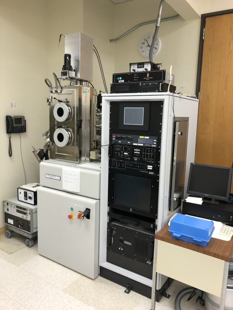
Electron beam evaporation is a physical vapor deposition (PVD) technique used to deposit high-purity thin films. In this process, a focused beam of high-energy electrons is directed onto a source material in a vacuum chamber, causing it to melt and evaporate. The resulting vapor condenses onto a substrate, forming a thin film. E-beam evaporation is ideal for materials with high melting points and allows for precise control over film thickness and composition. It is also ideal for situations where directional film deposition is essential, such as in lift-off processes. It is not suitable for processes requiring good sidewall coverage.
We can deposit a wide variety of materials using e-beam evaporation, including common metals such as paladium (Pd), ohmic contacts for III-V compound semiconductors such as nickel (Ni) / germanium (Ge) / gold (Au) or titanium (Ti) / platinum (Pt) / gold (Au), dielectrics such as titanium dioxide (TiO2), silicon dioxide (SiO2), aluminum oxide (Al2O3), tantalum pentoxide (Ta2O5), yttrium fluoride (YF3), and semiconductors such as silicon (Si). We have in-situ monitoring capabilities using crystal monitors and/or optical thickness monitors, and we can heat samples during deposition to improve film density.
| E-Beam Evaporation | Thermal Evaporation | Sputtering | |
|---|---|---|---|
| Deposition Mechanism | Electron beam heats and evaporates target | Resistive heating evaporates target | Ion bombardment ejects atoms from a target |
| Material Suitability | High-melting-point and refractory materials | Low to moderate melting-point materials | Wide range, including metals, dielectrics, and alloys |
| Film Density | Moderate, better than thermal but less than sputtering | Low, porous and less dense | High-density, uniform films |
| Adhesion Quality | Good, but better with adhesion layer | Often poor without adhesion layer | Generally strong adhesion due to energetic deposition |
| Deposition Rate | Moderate to high | High | Moderate to low |
| Film Purity | High | High, but more risk of contamination from heating elements | Lower due to gas incorporation and potential for target contamination |
| Step Coverage | Moderate | Moderate in one SRI system. Anisotropic in another | Good step coverage, suitable for 3D features |
| Process Complexity | Moderate (requires e-beam source and cooling) | Simple | Complex (plasma control, target biasing, reactive gases) |
| Reactive Deposition | Available in SRI system | No | Available in SRI systems (e.g., reactive sputtering to deposit oxides or nitrides) |
| Substrate Heating | Moderate | Low to moderate depending on material | Significant due to plasma and ion impact |
Low Pressure Chemical Vapor Deposition (LPCVD)
LPCVD is a chemical vapor deposition technique used to deposit high-quality, uniform thin films on substrates in a low-pressure environment (typically 0.1–1 Torr). In this process, precursor gases react or decompose at elevated temperatures (usually 400 – 900°C) in a tube furnace, forming a solid film on the substrate surface. Operating at low pressure improves film uniformity, purity, density, and step coverage, as well as reduces gas-phase particle formation.
We offer LPCVD amorphous silicon (a-Si), polysilicon (poly-Si), silicon dioxide (SiO2), dopant implant activation, and associated processes, such as thin film transistors.
Plasma-enhanced Chemical Vapor Deposition (PECVD)
PECVD is a low-temperature chemical vapor deposition technique that uses plasma to enhance chemical reactions at the substrate surface, enabling thin film deposition at much lower temperatures (typically 150–400°C) compared to traditional CVD processes. The plasma is generated by applying radio frequency (RF) or microwave power to a low-pressure gas mixture, creating reactive species (ions and radicals) that drive film formation. PECVD films are good candidates for forming electrically insulating layers on structures or devices that cannot sustain high temperatures.
We offer PECVD amorphous silicon (a-Si), silicon nitride (Si3N4), silicon dioxide (SiO2), and silicon oxinitride (SiON), including multi-stacked doped a-Si to form photodetectors and thin film transistors (TFTs)
Metal Organic Chemical Vapor Deposition (MOCVD)
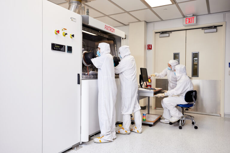
MOCVD is a specialized form of chemical vapor deposition used to grow high-quality compound semiconductor single crystal thin films, particularly III-V materials such as gallium arsenide (GaAs), indium phosphide (InP), and gallium nitride (GaN). In MOCVD, metal-organic precursors (trimethylgallium, trimethylaluminum, trimethylindium) and hydride gases (arsine, phosphine, ammonia) are introduced into a heated reaction chamber, where they decompose and react at the substrate surface to form a crystalline film.
Complex multi-layers of compound semiconductor alloys with atomically abrupt interfaces can be epitaxially grown on a lattice-matched substrate to form devices such as laser diodes, LEDs, photodetectors, and power amplifiers. The technique allows for atomically precise control over material composition, film thickness, and doping, enabling development of heterostructures with unique electronic and optical properties through bandgap engineering.
We offer MOCVD capabilities in wide-bangap (GaN and associated InAlGaN heterostructures) and ultra-wide bandgap (AlN and associated AlGaN heterostructures), including established blue, violet, and UV LEDs and laser diode epilayers.
We also offer MOCVD capabilities in GaAs, GaSb, and InP heterostructures, including devices like avalanche photodetectors.
“Being able to participate in the MOCVD growth, device fabrication, and characterization … directly is a great strength of the program in progress. I especially appreciate the detailed preparation and the execution by the PARC/SRI team members.”
S.R., Research Fellow, LED R&D Center
Client company manufacturer of mobile phone camera modules, automotive electronics, and semiconductor substrates
On the co-development of optoelectronic light-emitters.
Atomic Layer Deposition (ALD)
Atomic Layer Deposition is a vapor-phase thin film deposition technique that allows for atomic-scale control of film thickness and composition. It is based on self-limiting surface reactions, where precursor gases are introduced sequentially in a cyclic manner. Each cycle (e.g., trimethylaluminum, followed by water vapor) deposits a sub-monolayer of material, enabling extremely conformal and uniform coatings, even on high-aspect-ratio or 3D structures. This technique allows for conformal deposition of high quality ultrathin films of less than 100 nm.
We offer both thermal and plasma-enhanced ALD capabilities, including aluminum oxide (Al2O3) films. We can also do ALD silicon dioxide (SiO2), silicon nitride (Si3N4), HfO, ZnO.
Screen Print
Screen printing is a patterning technique used to deposit thick films of functional materials, such as solder, adhesives, inks, or pastes, onto flat or slightly curved substrates. A stencil that defines the pattern is aligned to features on an underlying substrate. The material is applied using a squeegee that forces it through the open areas of the stencil onto the substrate below. After deposition, the printed layer is typically dried, sintered, or melted to achieve the desired mechanical or electrical properties.
We offer capabilities on screen printing of solder paste and conductive epoxy for electronic component interconnect or for multi-substrate thru-hole bonding.
Electroplating
Electroplating is a metal deposition process in which a layer of metal is deposited onto a conductive surface using an electrochemical reaction. The process involves immersing the target substrate (the cathode) and a metal source (the anode) into an electrolyte solution containing metal ions. When an electrical current is applied between the anode and the substrate, metal ions in the solution flow toward the substrate, are reduced, and deposit onto the substrate, forming a metallic film on the electrically conductive portion of the substrate. This technique has the capability to form conductive films much thicker than physical or chemical vapor deposition (PVD or CVD) and does so in a low temperature process.
We offer both electro-less and electroplating capabilities with patterned films exceeding 140 microns thick. We have expertise fabricating interposers with electroplated interconnect lines and thru-vias. We also offer capabilities fabricating 3D Micro-Electro-Mechanical-Systems (MEMS) devices incorporating electroplated structures.
