
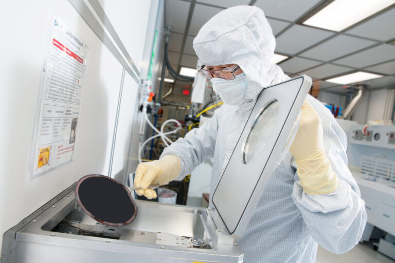
Description
Etching is a material removal process used to remove layers from a substrate to create patterns or structures. It is typically used after lithography to transfer a pattern into underlying films. Masking materials, such as photoresist or metal, protect defined regions from the process, while allowing exposed areas to react with process chemicals or gasses. Etching can be isotropic (uniform in all directions) or anisotropic (directional), depending on the technique and materials. Also, some processes can be made selective, where a target material is removed while leaving others intact even when both are exposed to the reactive elements.
What We Offer
We offer both wet chemical etching and dry etching. Wet etching involves using liquid chemicals to dissolve materials, while dry etching uses plasma or reactive gases, enabling fine control over sidewall profiles and aspect ratios.
Materials
We have capabilities on etching a wide variety of materials, including semiconductors like silicon (Si), gallium arsenide (GaAs), indium phosphide (InP), and gallium nitride (GaN) and their associated alloys. We also have etch processes for many metals, and we have extensive experience with dielectrics.
- Dielectric
- Metal
- Semiconductor
- Organics
Etching Techniques
Reactive Ion Etching (RIE)
Reactive Ion Etching (RIE) is a dry etching technique used to precisely remove material from a substrate by combining chemical reactions with physical ion bombardment. The process involves generating a plasma in a low-pressure chamber using reactive gases. A radio frequency (RF) electric field is also applied to accelerate ions toward the substrate surface. The ions physically bombard the substrate to dissociate materials, while the reactive species perform chemical etching, resulting in an efficient and anisotropic (directional) etching process.
We offer RIE capabilities utilizing various reactive gasses, including carbon tetrafluoride (CF4), fluoroform (CHF3), oxygen (O2), sulfur hexfluoride (SF6).
Deep Reactive Ion Etching (DRIE)
DRIE is a specialized form of reactive ion etching designed to create deep, high aspect ratio structures in silicon, while maintaining vertical, anisotropic sidewalls. The process involves rapidly cycling between an etching step using gases like SF6 to etch Si and a passivation step using gases like C4F8 to deposit a thin fluorocarbon polymer that coats and protects the newly formed sidewalls. The repeated etch and sidewall coating cycles enable formation of deep trenches and holes with smooth sidewalls.
We offer DRIE capabilities, useful for developing devices like Micro-Electro-Mechanical-Systems (MEMS) or Thru-substrate interconnects.
Inductively Coupled Plasma (ICP) Etching
ICP etching is a type of plasma etching technique used to achieve high etch rates, good anisotropy, and fine process control. It uses an RF-powered inductive coil to generate a dense plasma independently of the substrate bias, allowing separate control of ion density and ion energy, a key advantage over conventional Reactive Ion Etching (RIE) for achieving good sidewall profile and low substrate damage.
We offer ICP etching of dielectrics, metals, silicon, and compound semiconductors like gallium arsenide (GaAs), indium phosphide (InP) and gallium nitride (GaN). Our ICP capabilities include chlorine-based chemistries.
Chemically-Assisted Ion Beam Etching (CAIBE)
CAIBE is an advanced dry etching technique that combines physical ion bombardment with chemical reactivity to achieve precise, directional, and selective material removal. It is a variation of ion beam etching (IBE), in which a collimated ion beam (typically Ar⁺) physically sputters the surface. In CAIBE, a reactive gas (such as chlorine (Cl2), sulfur hexafluoride (SF6), or oxygen (O2)) is introduced simultaneously to enhance etching through chemical reactions at the surface, increasing the etch rate and selectivity.
We offer CAIBE capabilities and have established processes for gallium arsenide (GaAs) and gallium nitride (GaN). We can tilt the substrate relative to the ion beam to help form a desired sidewall profile. Our CAIBE experience includes forming etched laser diode facets and Micro-Electro-Mechanical-Systems (MEMS) comb drives.
Xenon Difluoride (XeF2) Etching
XeF2 etching is a dry, vapor-phase, isotropic etching technique for silicon. It relies on the spontaneous chemical reaction between xenon difluoride gas and exposed silicon surfaces, forming volatile byproducts such as silicon tetrafluoride (SiF4) and xenon (Xe), which are pumped away. The process occurs without plasma, making it gentle, selective, and clean.
The etching process is highly selective to silicon over other materials like SiO2 and SiN. It is particularly useful for sensitive devices or materials that are susceptible to plasma damage because the etch is performed at room temperature with no plasma or ion bombardment. The process is also useful for releasing Micro-Electro-Mechanical-Systems (MEMS) structures, where sacrificial silicon layers beneath suspended structures are removed. The process does not generate byproducts, making it contamination-free.
We offer XeF2 processing capabilities.

Wet Chemical Etching
Wet chemical etching is a material removal process in which solid materials are dissolved by liquid chemical solutions. It is used to pattern thin films or bulk substrates after photolithographic masking. Wet etching relies on chemical reactions at the surface, often aided by diffusion and temperature, to selectively remove exposed materials.
We have wide expertise on chemical etching and offer capabilities in wet etching of semiconductors, thin films, metals, dielectrics, and polymers. Our expertise includes anisotropic potassium hydroxide (KOH) etching of silicon to form either inverted pyramid structures or crystallographically-defined perpendicular sidewalls.