Description
Characterization refers to the set of analytical techniques used to measure, analyze, and verify the properties and performance of materials, structures, and devices fabricated during semiconductor and microfabrication processes. These techniques are essential for process monitoring, quality control, and research, ensuring that films, surfaces, and devices meet designed specifications.
What We Offer
We offer a comprehensive suite of techniques and tools for materials characterization, including scanning electron microscopy (SEM), high resolution x-ray diffraction (HRD), photoluminescence (PL), spectrophotometry, profilometry, atomic force microscopy, ellipsometry, and film stress analysis, among others. Our expert team in semiconductor development and microfabrication skillfully employs these methods to ensure that the materials, processes, and devices we develop for you deliver high performance, reproducibility, and fabrication yield.
Materials
- Thin Films
- Laser diodes
- Photodetectors
- Heterostructures
- Distributed Bragg Reflector (DBR)
Characterization Techniques
Scanning Electron Microscopy (SEM)
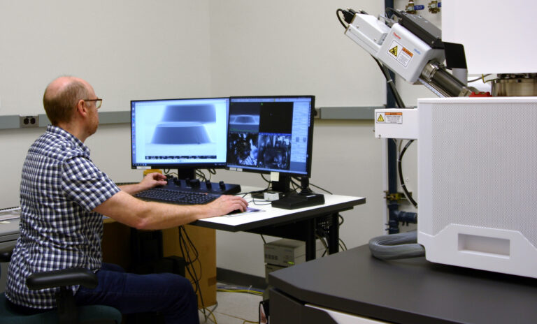
SEM is an imaging technique used to observe micro-structures, surface topography and composition with resolution down to the nanometer scale. The technique uses an electron beam to scan across the sample surface. When electrons interact with the sample, they generate secondary electrons for high magnification imaging. The exposure also produces backscattered electrons that can be used for compositional analysis, and x-rays that can be used for elemental analysis (EDS).
We provide SEM characterization as part of our materials and device fabrication process development services. Our SEM systems support multiple imaging modes and are equipped with energy-dispersive X-ray spectroscopy (EDS) for elemental analysis. These tools enable detailed inspection of microfabricated structures, etch profiles, critical dimensions, and cross-sections of multilayer films. EDS is used to identify material composition and investigate features such as plasma etch residues and particulate contaminants.

High Resolution X-Ray Diffraction (HRD)
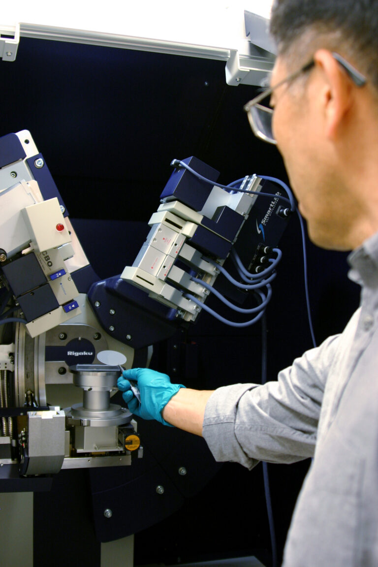
HRD is an analytical technique used to characterize the crystallographic properties of epitaxial layers, with extremely high angular precision. It is used to assess semiconductor crystal quality, strain, lattice constants, dislocations, and layer thicknesses. A monochromatic X-ray beam is directed at the sample at varying incidence angles. The X-rays diffract according to Bragg’s Law from the crystal planes of the material. A high-resolution detector and optics system precisely measures the intensity of diffracted beams as a function of angle to produce a rocking curve or reciprocal space map for analysis.

We provide HRD as part of our epilayer growth and heterostructure development services. Our analysis includes studying quantum well composition, layer thicknesses, and strain, as well as performing simulations.
Photoluminescence (PL)
PL is an optical characterization technique used to probe the electronic and optical properties of materials. When a material is excited with light from a laser it emits light at characteristic wavelengths. By analyzing this emitted light, PL spectroscopy provides information about bandgap energy, defect states, material quality, and impurity levels.
We provide PL as part of our epilayer growth and heterostructure development services. Our analysis includes evaluating semiconductor epitaxial layers and quantum wells to assess uniformity, detect defects, and monitor heterostructure quality.
Spectrophotometry
Spectrophotometry is an optical measurement technique used to quantify the transmission, reflection, and absorption properties of materials across a range of wavelengths, from the ultraviolet to the near-infrared spectrum. By analyzing how light interacts with a sample, spectrophotometry provides insights into film thickness, optical constants (refractive index and extinction coefficient), and material composition.
We provide spectrophotometry as part of our materials and device fabrication process development services. We use it to characterize thin films, coatings, and transparent or semi-transparent materials, such as anti-reflection and high reflectivity multi-stacks and Distributed Bragg Reflector (DBR) epilayer mirrors.
Thin Film Process Monitoring
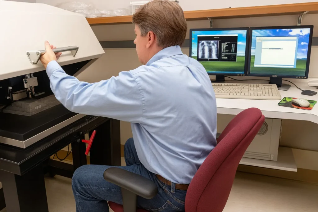
Our thin film process monitoring capabilities include profilometry, atomic force microscopy (AFM), ellipsometry, interferometry, sheet resistance, and film stress analysis. These characterization techniques enable monitoring of film thickness, etch depth, surface roughness, film quality, electrical resistivity, and film stress.
We provide these capabilities as part of our materials and device fabrication process development services to ensure high performance, reproducibility, and fabrication yield.
