Vertical-cavity Surface-emitting Lasers (VCSEL)
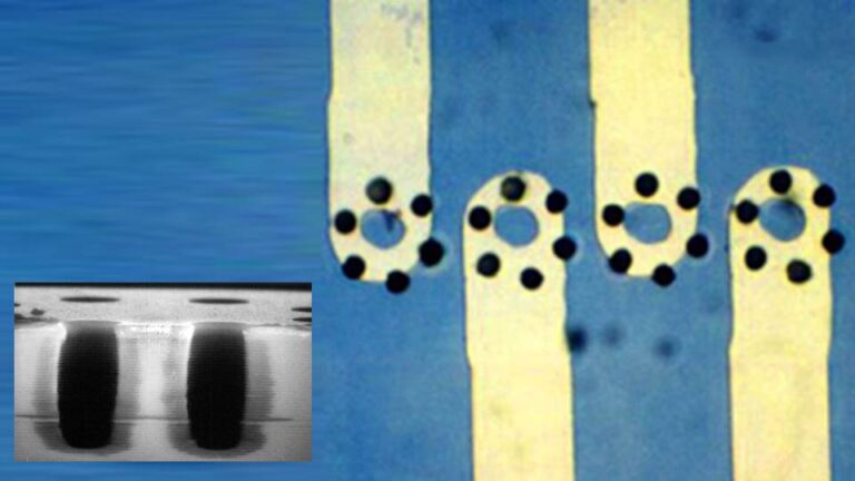
Special Features: Oxide-confined yet planar. Invented at SRI.
Impact: A large percentage of commercial high performance VCSELs have adopted this planar lateral oxide architecture because it enables manufacturability and dense packing.
VCSELs are widely used in datacenter links, mobile phone facial recognition systems, automotive lidar, and laser printing.
Relevant Process: Plasma Etching
On-chip High Q-factor Coils
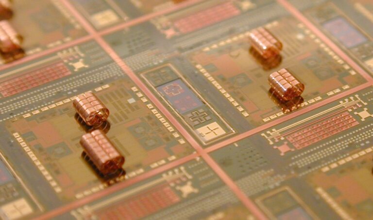
Special Features: Coil axis parallel to wafer plane ensures minimal detrimental magnetic field penetrates the wafer. Invented at SRI.
Impact: High Q-factor coils are highly desired in many RF integrated circuits. However, they are the only passive electronic component that cannot be easily integrated into ICs. This invention removed that bottleneck.
Relevant Process: Back-end-of-line microfabrication, Micro-Electro-Mechanical-Systems (MEMS), Thin film stress engineering
Photonic Integrated Circuit Micro-ring Resonator
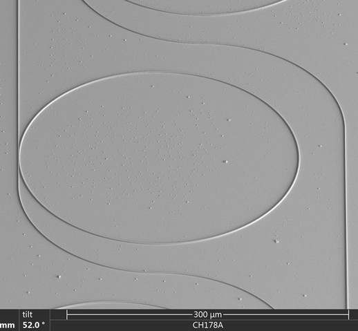
Special Features: Bus and ring waveguides fabricated out of epitaxial Aluminum Nitride (AlN) for blue/UV wavelength operation.
Impact: Development of PIC-based narrow linewidth compact UV semiconductor lasers for next generation optical atomic clocks.
Relevant Process: Plasma etching, epitaxial growth, facet optical coating, backend (polishing)
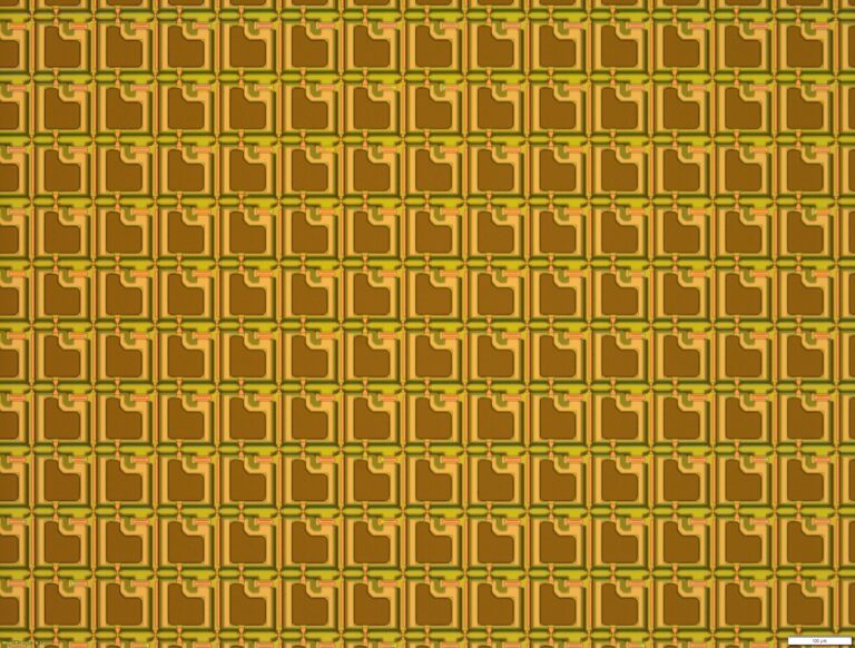
Thin Film Transistor Backplane
Special Features: Transistor circuits on glass or plastic, enabling direct fabrication of electronics on large area substrates and flexible materials.
Impact: Image scanner integrated on ultrasonic finger print sensor incorporated into smart phones by leading manufacturer. X-ray imager backplanes.
Relevant Process: Plasma-Enhanced Chemcial Vapor Deposition (PECVD) of doped semiconductors, transparent electrode technology (Indium Tin Oxide, or ITO)
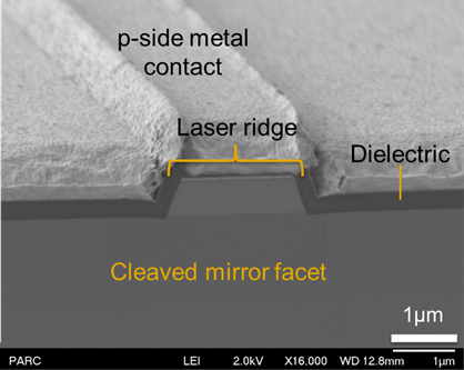
Blue/UV Semiconductor Lasers
Special Features: Full capability in design, growth and fabrication of wide bandgap InAlGaN laser diodes.
Impact: First in the United States, second in the world, to demonstrate a Gallim-Nitride (GaN)-based blue semiconductor laser.
Relevant Process: Metal Organic Chemical Vapor Deposition (MOCVD), plasma etching, metal alloy deposition and contact formation, backend (substrate thinning, facet cleaving)
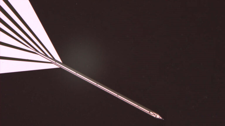
Micro-needle for magnetic neural stimulation
Special Features: Integrated micro-coil co-fabricated with silicon micro-needle for brain-implantable intracortical neural stimulation.
Relevant Process: Deep Reactive Ion Etching (DRIE), Micro-Electro-Mechanical-Systems (MEMS)
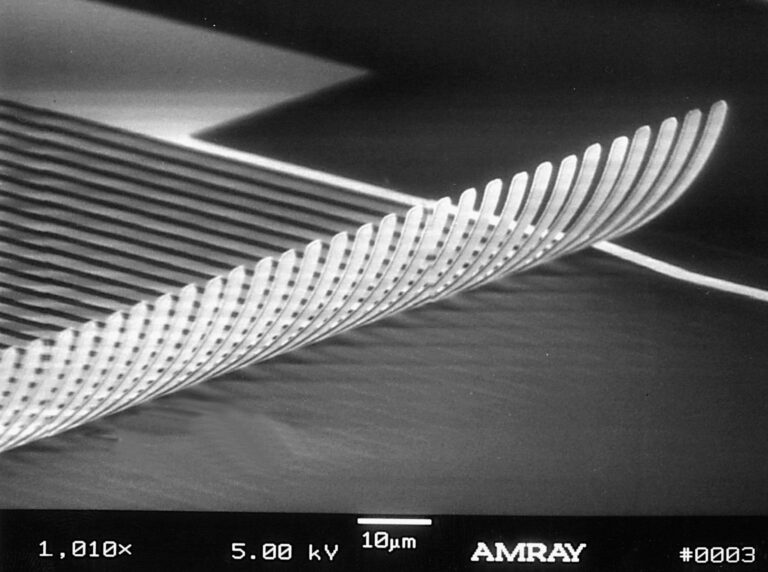
Micro-springs for probing and interconnecting of high density chip contact pads
Special Features: Microfabrication enables scaling of micro-probes to below 6 um pitch.
Impact: Remateable known-good-die testing of advanced chips. Wafer-level packaging with high tolerance to substrate non-planarity.
Relevant Process: Micro-Electro-Mechanical-Systems (MEMS), thin film deposition with precise stress engineering
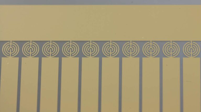
Gas sensors on flexible substrates
Special Features: Electrode arrays on flexible substrates with functionalized carbon nanotubes for gas sensing.
Impact: Low cost distributed gas sensing networks capable of detecting toxic gases, such as methane, ammonia, carbon monoxide, hydrogen sulfide
Relevant Process: Flexible electronics, Plasma-Enhanced Chemcial Vapor Deposition (PECVD) on plastic, metal deposition, patterning
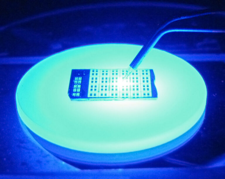
UV (325 nm) LED
Special Features: Complex heterostructure on sapphire comprising of metamorphically-grown AlGaN, bandgap engineered layers, and precisely-doped structures.
Impact: Commercial product introduction by partner for the adhesive curing and bioscience industries.
Relevant Process: Metal Organic Chemical Vapor Deposition (MOCVD), plasma etching of ultra-wide bandgap (UWBG) semiconductors
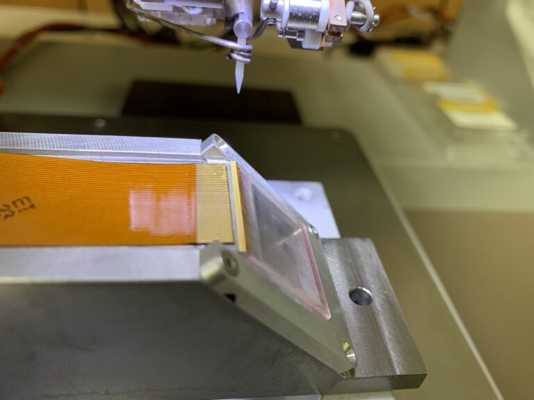
Chiplet Transfer Head
Special Features: Microfabricated heater arrays combined with shaped memory alloy films for mass transfer and selective pick and place of micro-LEDs or chiplets.
Impact: Ability to selectively pick and place large number of small, fragile chiplets the size of red blood cells spaced less than 5 um apart for the micro-LED and chiplet ecosystem.
Relevant Process: Thin film deposition, backend
