
Description
MOCVD is a specialized form of chemical vapor deposition used to grow high-quality compound semiconductor single crystal thin films, particularly III-V materials such as gallium arsenide (GaAs), gallium antimonide (GaSb), indium phosphide (InP), and gallium nitride (GaN). In MOCVD, metal-organic precursors (trimethylgallium, trimethylaluminum, trimethylindium) and hydride gases (arsine, phosphine, ammonia) are introduced into a heated reaction chamber, where they decompose and react at the substrate surface to form a crystalline film.
Complex multi-layers of compound semiconductor alloys with atomically abrupt interfaces can be epitaxially grown on a lattice-matched substrate to form devices such as laser diodes, LEDs, photodetectors, and power amplifiers. The technique allows for atomically precise control over material composition, film thickness, and doping, enabling development of heterostructures with unique electronic and optical properties through bandgap engineering.
What We Offer
We offer custom MOCVD epitaxial growth of compound-semiconductor heterostructures tailored to your needs and designs. We work closely with you to understand your objectives, and we apply our knowhow developed over decades of experience toward your project. The end products are epilayer wafers and associated characterization data.
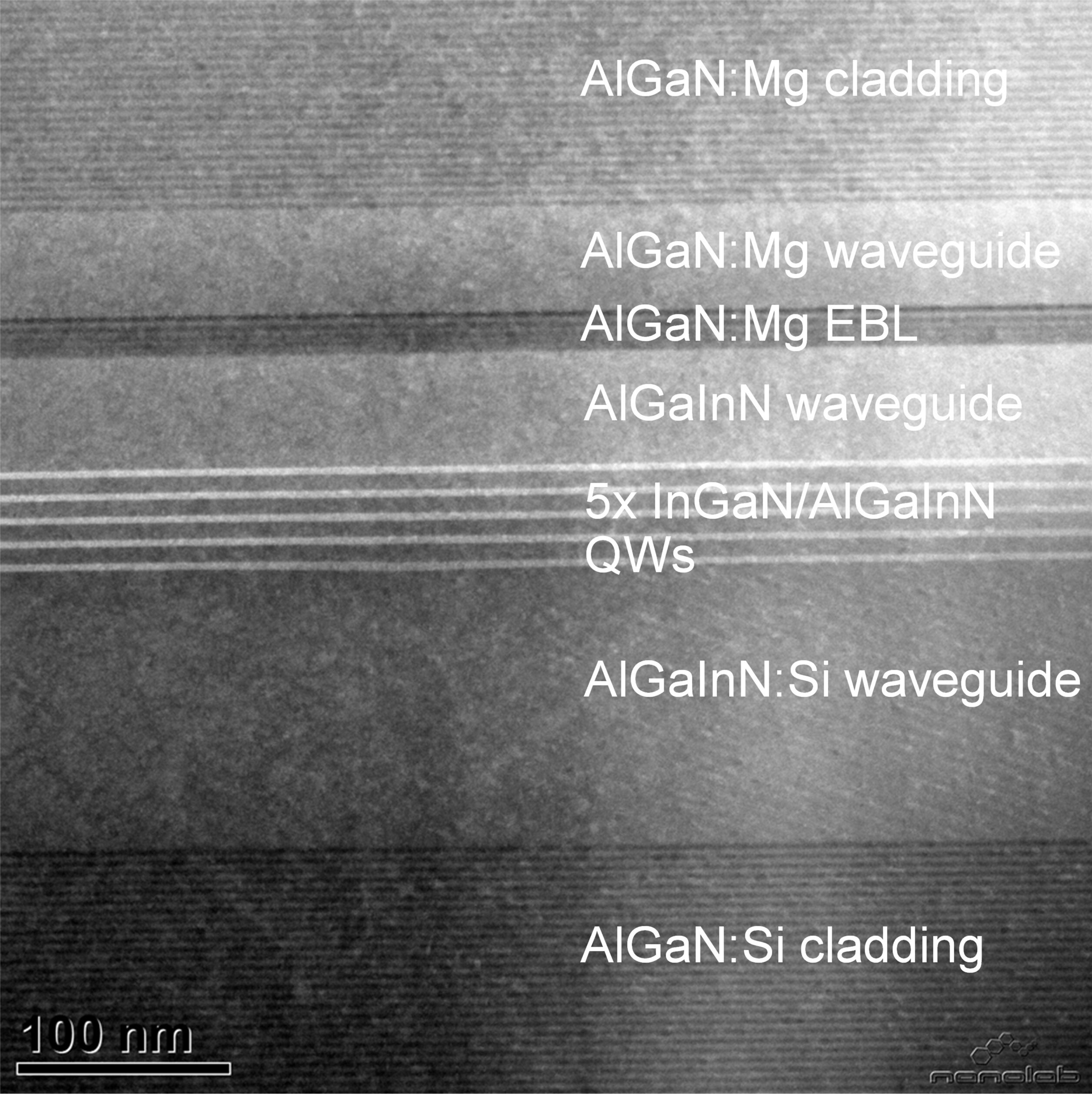
Materials
| Material System | Ternaries | Quaternaries | p-dopant | n-dopant |
|---|---|---|---|---|
| GaAs | AlGaAs, InGaAs, InGaP | InGaAsP, InAlGaP | Zn, C | Si, Te |
| InP | InGaAs, InAlAs, GaAsSb | InGaAsP, InAlGaAs | Zn, C | Si, Te |
| GaSb | InAsSb, AlGaSb | InGaAsSb, AlGaAsSb, InAsSbP | Zn, C | Si, Te |
| GaN Substrates: Bulk GaN or Sapphire | InGaN, AlGaN | InAlGaN | Mg | Si |
| AlN Substrates: Bulk AlN or Sapphire | InGaN, AlGaN | InAlGaN | Mg | Si |
We can perform wafer-scale Zn diffusion, epitaxial regrowth, and Fe-doped semi-insulating InP regrowth.
Example device epilayers include Fabry Perot laser diodes (Red, IR, blue and UV (369 nm)), LEDs, VCSELs, PIN photodiodes, Avalanche photodetectors, thermophotovoltaics.
“Being able to participate in the MOCVD growth, device fabrication, and characterization … directly is a great strength of the program in progress. I especially appreciate the detailed preparation and the execution by the PARC/SRI team members.”
S.R., Research Fellow, LED R&D Center
Client company manufacturer of mobile phone camera modules, automotive electronics, and semiconductor substrates
On the co-development of optoelectronic light-emitters.
