Description
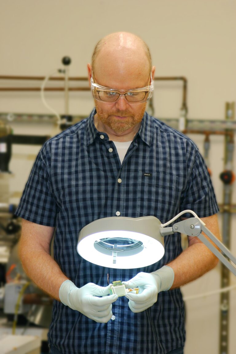
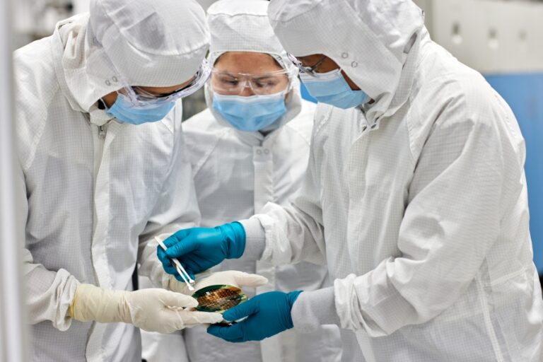
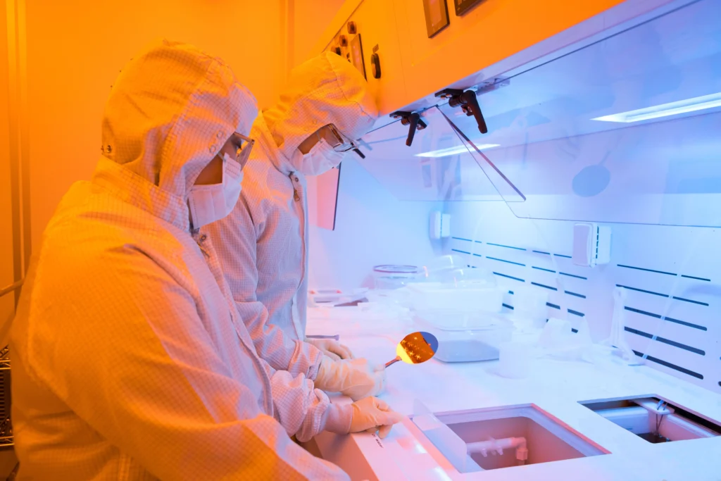
We provide end-to-end custom microfabrication process development services, tailored to meet the unique requirements of advanced device concepts. Our team works closely with clients to translate ideas into robust, reproducible process flows, combining expertise in thin film deposition, photolithography, etching, and packaging. Whether the goal is to demonstrate proof-of-concept devices, refine integration steps, or scale toward pilot production, we design and optimize each process module with precision and repeatability in mind.
What We Offer
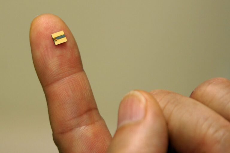
Our capabilities span both front-end and back-end of line integration, enabling us to fabricate custom structures on foundry Complementary Metal Oxide Semiconductor (CMOS) wafers or build from the substrate up. We support development across a wide range of materials—including semiconductors, glass, dielectrics, polymers, and metals—and leverage advanced characterization tools to validate every stage.
Process development is carried out iteratively, with in-line metrology and electrical/mechanical characterization feeding back into design refinements. This ensures tight process control and early identification of failure modes. We also address integration challenges such as stress management in multilayer stacks, step coverage in high aspect ratio features, and interface engineering for heterogeneous materials. Our goal is to deliver well-documented, transferable process flows that allow clients to transition smoothly from laboratory prototypes to pilot-scale fabrication.
By offering flexible engagement models, from feasibility studies to full process transfer, we help clients accelerate innovation while reducing technical risk.


