Description
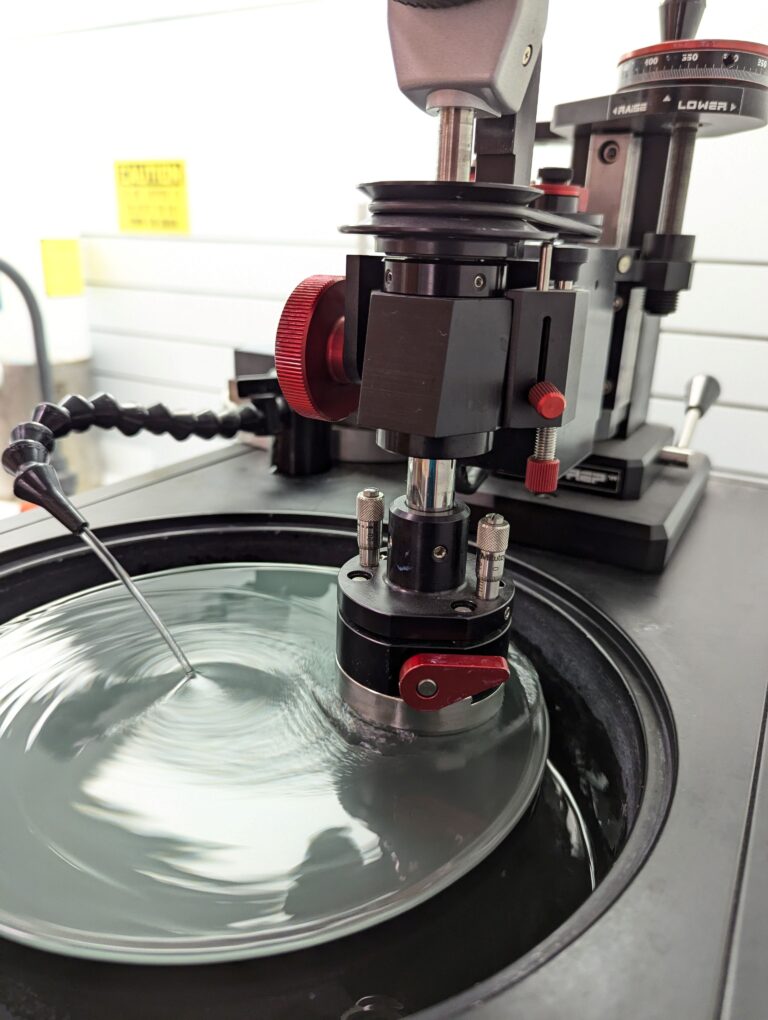
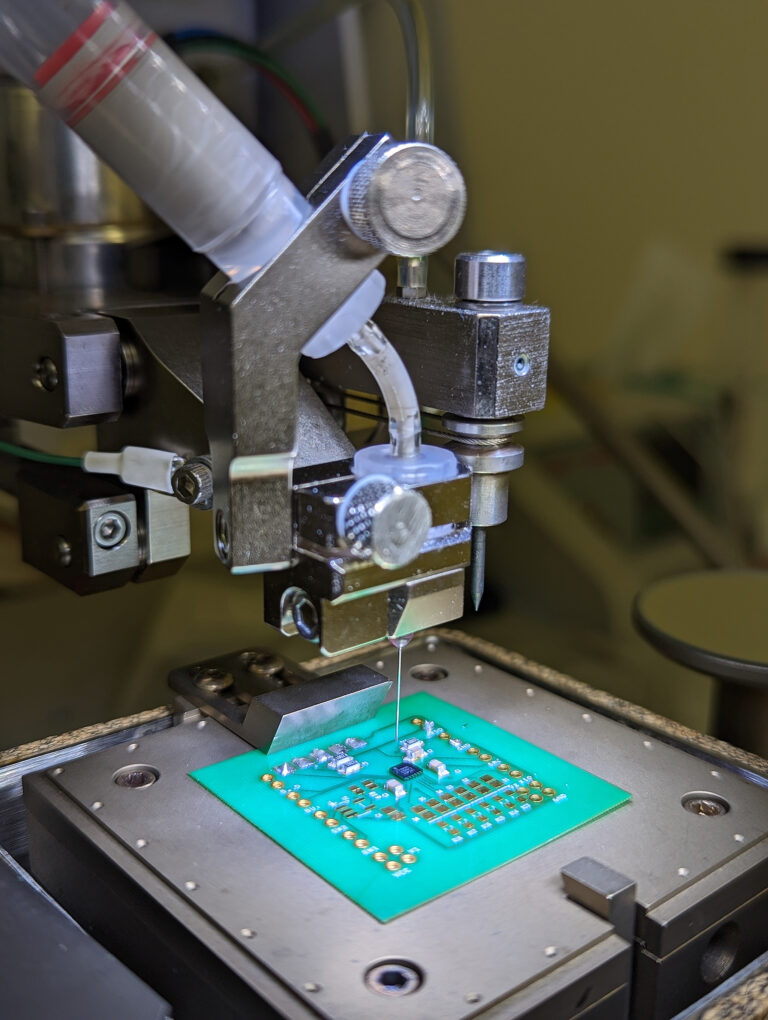
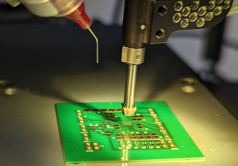
Backend microfabrication encompasses the final stages of semiconductor and device processing, typically occurring after front-end device formation. These processes include substrate thinning, wafer polishing, cleaving, dicing, wire bonding, die attach, flip-chip assembly, small die handling. These processes are critical for enabling functional integration and packaging for system-level performance.
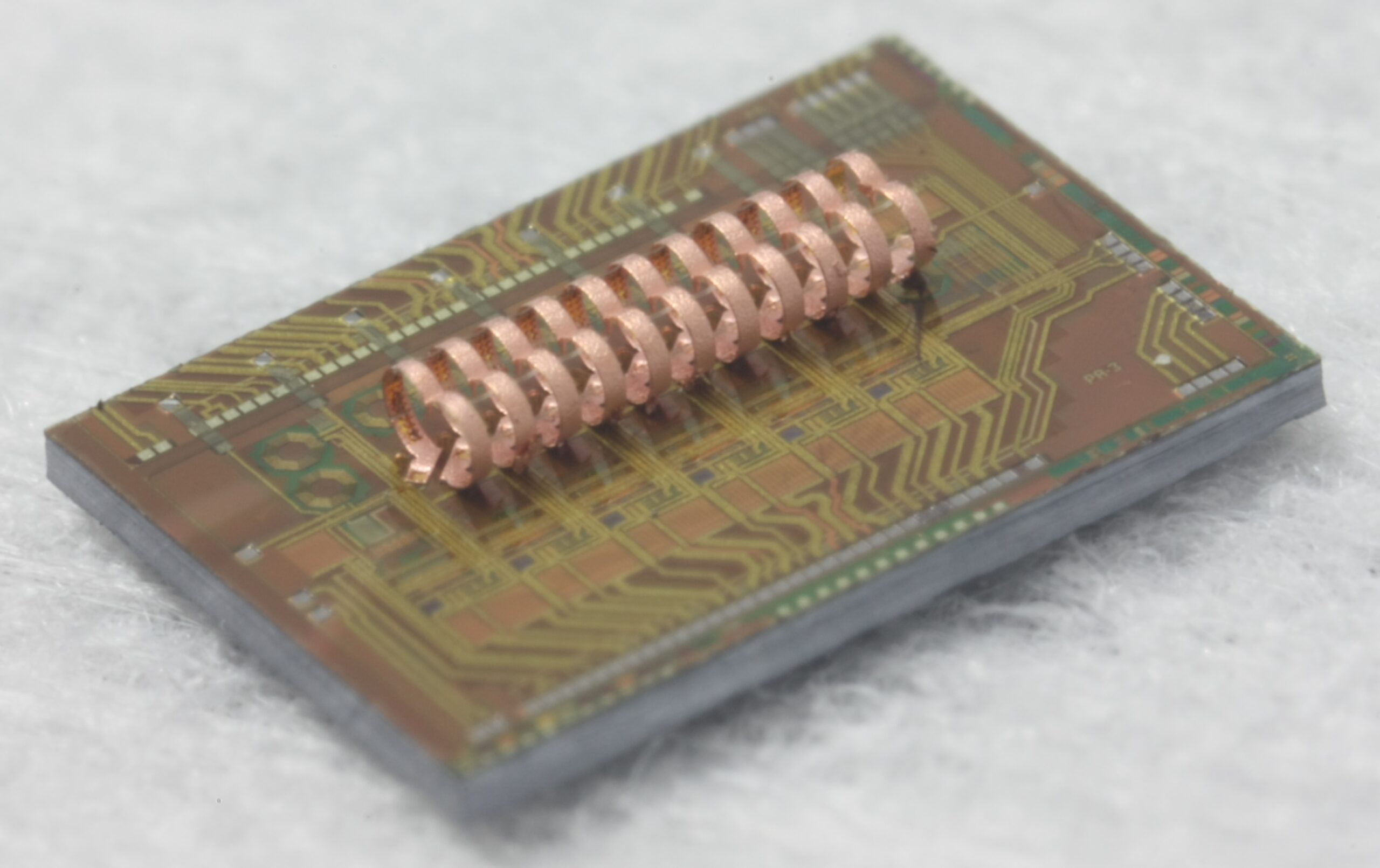
We also perform add-on back-end-of-line fabrication on Complementary Metal Oxide Semiconductor (CMOS) foundry wafers. Processes include redistribution lines, interlayer dielectrics, opening buried bond pads on wafer-bonded structures, selective area optical coating, and excimer laser shallow dopant activation.
What We Offer
We offer backend capabilities important for Micro-Electro-Mechanical-Systems (MEMS), photonics, and microelectronics. Our expertise includes thinning substrates such as silicon (Si), gallium arsenide (GaAs), indium phosphide (InP)), gallium nitride (GaN), and sapphire. We can cleave compound semiconductors to form mirror facets, and we can polish edges of cut substrates such as sapphire to form waveguide input/output optical couplers for photonic integrated circuits. We have capabilities for die attach, including flip-chip ball grid array interconnect, and we have capabilities to pick and place micron-size chiplets such as micro-LEDs.


“It was a pleasure to work with the SRI/PARC team as they developed back-end-of-line post-CMOS microfabrication processes to integrate novel, high-performance RF MEMS on custom CMOS wafers. From designing the MEMS structures and modeling their electrical and mechanical properties, to crafting photomask layouts and fabricating thin-film devices and interlayer dielectrics at their microfabrication facility, the team’s technical expertise shone through at every step. They worked hand-in-hand with our team’s RF circuit specialists, foundries, and microelectronics vendors to ensure everything came together seamlessly. Throughout the project, they provided clear, meticulous updates, hit challenging milestones with ease, and consistently went above and beyond expectations. I cannot recommend them enough and look forward to working again with them on a future endeavor.”
Project Manager
Client company manufacturer of smart phones
On a project developing novel RF communication links for mobile phones.

