Film Deposition
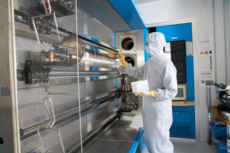
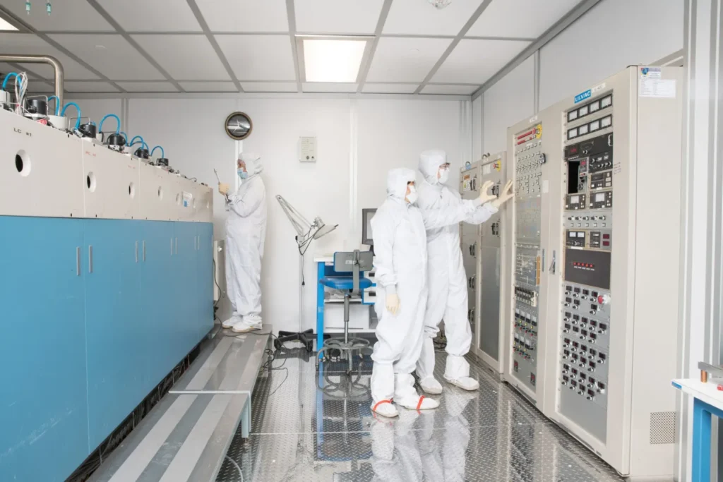
We offer comprehensive thin film deposition services. Whether you require simple single-layer films on your chosen substrate or process development to determine the optimal materials and methods for your device, we can support you at every stage.
Materials:
Dielectric
Metal
Solder
Semiconductor
Processes:
Physical Vapor Deposition (PVD; Sputtering)
E-Beam Evaporation
Thermal Evaporation
Low Pressure Chemical Vapor Deposition (LPCVD)
Plasma-Enhanced Chemical Vapor Deposition (PECVD)
Metal Organic Chemical Vapor Deposition (MOCVD)
Atomic Layer Deposition (ALD)
Screen Print
Electroplating
Etching
We offer both wet chemical etching and dry etching, and have capabilities on etching a wide variety of materials, including semiconductors like Silicon (Si), Gallium Arsenide (GaAs), Indium Phosphide (InP), and Gallium Nitride (GaN) and their associated alloys.
Materials:
Dielectric
Metal
Semiconductor
Organics
Processes:
Reactive Ion Etching (RIE)
Deep Reactive Ion Etching (DRIE)
Inductively-Coupled Plasma (ICP)
Chemically-Assisted Ion Beam (CAIBE)
Xenon Difluoride (XeF2)
Wet Chemical
Patterning
We offer a wide range of techniques and materials for patterning. Our capabilities include photolithography and shadow masking.
Materials:
Photoresist
SU-8
Benzocyclobutene (BCB)
Polyimide
Processes:
Photolithography
Ebeam Lithography
Dry Film Processing
Lift-Off Processing
Characterization
We offer a comprehensive suite of techniques and tools for materials characterization, including Scanning Electron Microscopy (SEM), High resolution X-Ray Diffraction (HRD), Photoluminescence (PL), spectrophotometry, profilometry, atomic force microscopy, ellipsometry, and film stress analysis, among others.
Materials:
Thin Films
Laser diodes
Photodetectors
Heterostructures
Distributed Bragg Reflector (DBR)
Processes:
Scanning Electron Microscopy (SEM)
X-Ray Rocking Curve
Atomic Force Microscopy (AFM)
Step Profilometry
Film Stress
Ellipsometry
Interferometry
Photoluminescence (PL)
Diode LIV
Film Resistivity
Spectrophotometer
Backend Microfabrication
We offer backend capabilities including wafer thinning, cleaving along substrate crystal planes to form edge facet reflectors, PIC edge coupler polishing, die attach, flip chip BGA interconnect, and selective pick & place of small chiplets and micro-LEDs. We also perform add-on back-end-of-line fabrication on post-Complementary Metal Oxide Semiconductor (CMOS) foundry wafers.
Learn MoreCustom Process Development
We provide end-to-end custom microfabrication process development services, tailored to meet the unique requirements of advanced device concepts. Whether the goal is to demonstrate proof-of-concept devices, refine integration steps, or scale toward pilot production, we design and optimize each process module with precision and repeatability in mind.
Learn More“Being able to participate in the MOCVD growth, device fabrication, and characterization … directly is a great strength of the program in progress. I especially appreciate the detailed preparation and the execution by the PARC/SRI team members.”
S.R., Research Fellow
LED R&D Center, Client company manufacturer of mobile phone camera modules, automotive electronics, and semiconductor substrates
On the co-development of optoelectronic light-emitters.

