
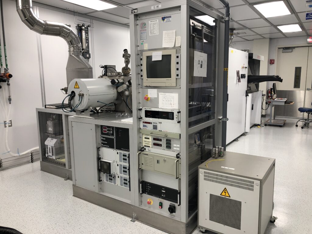
Equipment


Thin Film Deposition
- Plasma-Enhanced Chemcial Vapor Deposition (PECVD) – single chamber
- Plasma-Enhanced Chemcial Vapor Deposition (PECVD) – multi-chamber, doped materials
- Low Pressure Chemical Vapor Deposition (LPCVD)
- Atomic Layer Deposition (ALD)
- Sputtering – multiple machines for different materials & configurations
- eBeam Evaporator
- Metal Organic Chemical Vapor Deposition (MOCVD) for III-V semiconductor heterostructure (gallium arsenide – GaAs, indium phosphide – InP, gallium nitride – GaN)


Photolithography
- Contact aligners
- Oxygen (O2) Plasma for descum and photoresist ashing
- Photoresist wet processing stations (spinning, developing, stripping)
- Lift-off stations
- Baking, Hexamethyldisilazane (HMDS), and ammonia (NH3) image reversal Ovens
- Photomask cleaning

Etching
- Chemically-Assisted Ion Beam (CAIBE)
- Inductively-coupled Plasma (ICP)
- Reactive Ion Etcher
- Xenon Difluoride (XeF2) Plasma-less etcher


Thermal Processing
- Various furnaces with controlled ambient
- Vacuum ovens with programmable temperature profiles
- Rapid Thermal Anneal
- Hydrogenation – passivation of processed silicon
- Excimer laser for shallow dopant activation and for forming Low Temperature Polysilicon (LTPS)
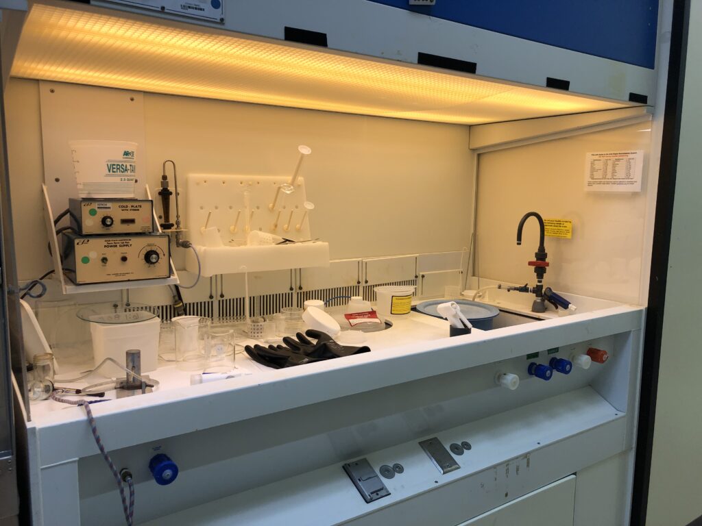

Wet Processing
- Various wet bench stations for specialized wet processes
- Electroplating
- Spin rinse dryers – 4”, 6”, 8”


Characterization
- Ellipsometer
- Interferometer
- Probe stations
- Profilometer
- Wafer bow film stress measurement
- Spectrophotometer
- Atomic Force Microscope
- Scanning Electron Microscope


Packaging
- Wafer backgrind and polishing
- Dicing saw
- Laser bar cleaver
- Die attach pick and place
- Wire bonder
- Flip-chip aligner


Epitaxial Growth
- Gallium Arsenide (GaAs) heterostructure
- Gallium Antimonide (GaSb) heterostructure
- Indium Phosphide (InP) heterostructure
- Gallium Nitride (GaN) heterostructure
- Aluminum Nitride (AIN) / Aluminum Gallium Nitride (AIGaN) heterostructure